1
/
of
5
METICULAB
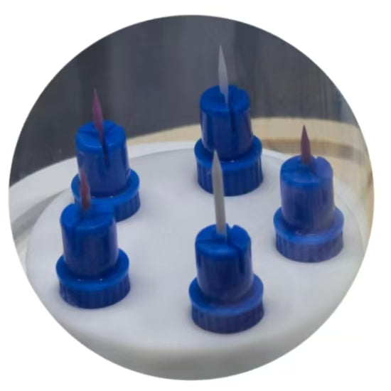
Meticulab High Precision Ceramic Bonding Capillaries for Semiconductor Packaging
Meticulab High Precision Ceramic Bonding Capillaries for Semiconductor Packaging
Quantity
Meticulab high-precision ceramic bonding capillaries are core consumables developed for semiconductor wire bonding processes, ideal for IC packaging, LED packaging, and discrete device applications. Designed to work with gold, copper, and silver wires, these capillaries offer tight dimensional tolerances and customizable surface roughness for reliable bonding performance.
📋 Product Series Specifications
|
Series
|
Tip Size
|
Hole/CD Tolerance
|
Recommended Wire
|
Typical Applications
|
|
Standard Type
|
60~100μm
|
±2~3μm
|
Gold Wire
|
LED Packaging, Discrete Devices
|
|
High-Performance Type
|
40~80μm
|
±1~2μm
|
Gold/Silver/Copper Wire
|
Power Management ICs, Memory Chips
|
|
Precision Type
|
20~50μm
|
±1μm
|
Ultra-Fine Gold/Copper Wire
|
Advanced Packaging, RF Chips
|
|
Custom Type
|
Customized based on pad size, wire loop shape, and surface roughness requirements
|
|||
⚙️ Core Technical Parameters
-
Tip Precision: ±1~3μm
-
Hole/CD Precision: Inner hole & inner chamfer 1~2μm
-
Surface Roughness: Ra 0.02~2.0μm
-
Material Hardness: HV 1800~2100
✅ Key Advantages
-
High Consistency: Batch-to-batch dimensional variation ≤±2μm, TIR <3μm for stable bonding yield
-
Long Service Life: High-hardness ceramic formulation and optimized tip design for enhanced wear resistance
-
Wide Process Window: Adjustable surface roughness to accommodate different wires and pad materials
-
Full Process Control: Domestic production closed-loop from powder, blanking, grinding to inspection
📌 Application & Selection Guide
-
Gold Wire Standard Bonding → Standard Type: Cost-effective, compatible with ASM/KNS and other mainstream bonders
-
Copper/Silver Wire High Reliability → High-Performance or Precision Type: Ultra-tight tolerances to reduce cratering
-
Special Pads or Fine Pitch → Custom Type: Tailored FA/CA/CD design
-
Existing Import Capillaries → We offer cross-referenced dimensions for direct drop-in replacement
Each Meticulab bonding capillary undergoes full AOI inspection and key dimension testing, with batch measurement reports available. Our technical team has over 15 years of wire bonding process experience, providing capillary selection, parameter optimization, troubleshooting, and application training for major bonder models.
🛠️ Service & Support
-
Sample verification available (7-day lead time)
-
Free selection consultation and technical guidance
-
Long-term supply agreements for bulk orders
-
Confidentiality agreements available for custom projects
📐 Customization Options
Customize tip size, inner hole (Hole), inner chamfer (CD), cone angle (CA), face angle (FA), and surface roughness. Specialized designs for gold, copper, silver, and aluminum wires to fit IC, LED, and discrete semiconductor packaging processes.
⭐ Custom Service Features
Professional engineers provide selection support, fast drawing/sample confirmation, and pre-production verification to reduce trial costs. We maintain stable lead times and consistent quality for mass production.
📋 Custom Process
-
Requirement Communication
-
Proposal Confirmation
-
Sample Production
-
On-Machine Verification
-
Mass Production
-
On-Time Delivery
Sample lead time: 7 working days | Bulk order lead time: 15-20 working days
🏭 Supply Capability
Long-term stable supply with strict dimensional and quality control. Trusted by semiconductor packaging, LED packaging, and discrete device manufacturers for high consistency and yield, even for large-volume orders.
Note: Neutral technical description, third-party testing supported. Direct supply, contact us for inquiries!
📩 Contact Us
📧 Email: choikyuc@gmail.com
📞 PhoneKakaoTalk ID: +82-10-3988-4813
💬 Click to WhatsApp
Korea‑Based Global Supplier | OEM & NDA Supported | R&D‑Driven Customization
Share